Single Event Latch-Up (SEL)
Latch‑up is a phenomenon in which a low‑impedance path suddenly forms between power and ground and persists even after the triggering event disappears. SEL differs in that its trigger is ion‑induced charge. Because the initial conditions of SEL are much harsher than those of an external voltage transient, even devices that are robust against general latch‑up require separate verification for SEL. Single Event Latch‑up (SEL) is a phenomenon in which high‑energy particles (primarily heavy ions) generate excess charge inside a device within a very short time (picoseconds, ps) and turn on a parasitic PNPN structure (parasitic thyristor) through a regenerative feedback mechanism. Once triggered, a low‑impedance, high‑current state persists until power is removed, which can cause anything from loss of functionality to destructive damage.
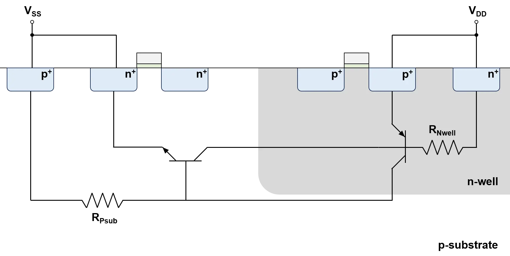
Parasitic PNPN (SCR) equivalent model of CMOS latch-up path including well/substrate resistance
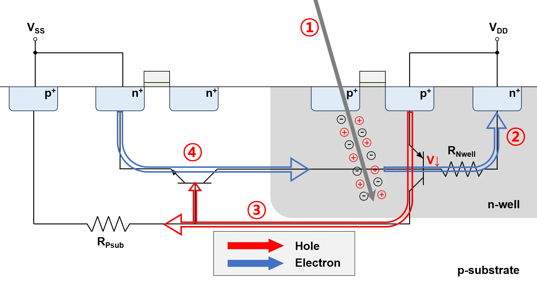
Turn-on sequence of the parasitic PNPN structure induced by heavy ions
① When a heavy ion or other high-energy particle penetrates the n-well, a large number of electron–hole pairs are instantaneously generated along the collision path (picoseconds–nanoseconds).
Immediately after generation, charges are collected by drift due to the electric field at the junction surface; electrons move mainly toward the n-well, and holes move mainly toward the p-substrate. This injected current causes a voltage drop (Δ𝑉=𝐼⋅𝑅) across the n-well resistance RNwell and the p-substrate resistance RPsub.
② While the majority carriers of the n-well, electrons, are collected at the n-well tap (n+ well contact connected to VDD), the voltage drop across RNwell lowers the local n-well (base) potential relative to VDD. If this potential difference becomes large enough to forward-bias the junction between P+ and the n-well (E-B of the parasitic vertical PNP), the PNP turns on first and injects holes from P+ (emitter) to the p-substrate (collector). (The P+ source/drain of the PMOS serves as the emitter of this PNP.)
③ The hole current flowing into the p-substrate (base) exits through the p+ substrate tap (connected to VSS), creating an additional voltage drop due to RPsub. At this time, if the p-substrate (base) potential rises above the local n+ (emitter, near VSS), the E-B of the parasitic lateral NPN is forward-biased and the NPN turns on,
④ Electrons are injected from the n+ emitter into the p-substrate (base) and collected into the n-well (collector) (the observed current flows in the direction from the collector (n-well) to the emitter (n+)). This increases the n-well current and the voltage drop across RNwell, which in turn further strengthens the forward bias of the PNP, forming a feedback structure.
The device that turns on first can be PNP or, depending on conditions, NPN (depending on the ion’s LET/trajectory, strike location, tap density, etc.). In either case, the parasitic PNPN structure is activated.
Turn-on stage of the PNPN structure
Factors affecting the turn-on of the parasitic PNPN structure
- Particle physics (primary factor): The ion species, LET (linear energy transfer), and trajectory determine the amount and spatial distribution of charge generated in the sensitive region. The higher the LET, the more charge is injected and the higher the probability of SEL occurrence. Larger induced current leads to larger induced voltage, increasing the likelihood of forming an E-B forward bias.
- Doping/resistance: The lower the substrate/well doping, the higher the sheet resistance, so the same charge creates a larger ΔV, lowering the turn-on threshold charge.
- Guard ring/tap spacing: The farther the generation point of electron–hole pairs is from the nearest tap, the larger the path resistance becomes, making the parasitic BJTs turn on more easily.
- Operating voltage: The higher the VDD, the larger the voltage across each resistance, making SEL possible with less charge.
- Temperature: Temperature rise generally reduces BJT turn-on voltage and increases β (bipolar gain), accelerating turn-on and increasing the gain product, thereby raising the likelihood of SEL.
SEL is a fatal error that does not recover until power is cut off. Even if it does not appear externally, potential damage such as metal melting, microcracks, and electromigration can occur, leading to reduced lifetime. In severe cases, the device can be destroyed by thermal runaway due to large current. Therefore, SEL evaluation is essential for devices operated in environments exposed to radiation such as space, aviation, accelerators, and high altitude. In addition, general latch-up robustness cannot guarantee SEL robustness, so heavy-ion evaluation is required.
QRT’s SEL evaluation/analysis services
- Heavy-ion–based SEL evaluation: We support derivation of threshold LET/cross-section parameters that comply with standards and verification of reproducibility.
- Pulsed laser–based evaluation: High–spatial-resolution local sensitivity mapping and source location estimation provide pre-screening/improvement guidance before beam time.
- System protection evaluation board design and evaluation: Design of supply current surge monitoring + high-speed cutoff/reset path and evaluation with optimized thresholds/delays.
- Failure analysis linkage: Identify potential defects such as metal extrusion/bridges and insulation cracks.
Related Articles
- Overview of Key Simulators for Radiation Effects Evaluation in Semiconductors
- How Was SEU Discovered? A Historical Insight into Radiation-Induced Failures in Electronic Circuits
- Energy Transfer Mechanisms of Ions
- Energy Transfer Mechanisms of Protons and Neutrons
- Energy Transfer Mechanisms of Electrons
- Energy Transfer Mechanisms of Photons
- Korean Radiation Test Facilities