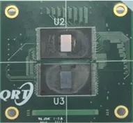
QRT’s laser evaluation system supports a wide wavelength range from 650 nm to 1650 nm, enabling radiation testing of a variety of semiconductor materials-such as silicon (Si), gallium nitride (GaN), and silicon carbide (SiC)-and device types including memories, processors, and analog components.
However, for certain 3D-stacked packages such as HBM (High Bandwidth Memory), the stacked architecture prevents sufficient laser access to the die, making complete evaluation infeasible.
Even outside such cases, feasibility can be constrained by the package’s structural characteristics.
A key prerequisite for laser evaluation is decapsulation-removal of the epoxy mold compound from the package. This must be performed with high precision to preserve test accuracy and reliability.
Devices with simple structures (e.g., amplifiers, ADCs, digital isolators) can typically be evaluated from both the front side and back side.
By contrast, highly integrated devices such as FPGAs, MCUs, SRAMs, and DRAMs generally require back-side-only evaluation because front-side metal stacks block laser penetration.
To determine feasibility in a specific case, it is best to consult prior case studies with similar structures.
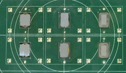
Evaluatable Package Types
Packages with structures like the one below are generally straightforward to decapsulate from both sides, making them suitable for evaluation.
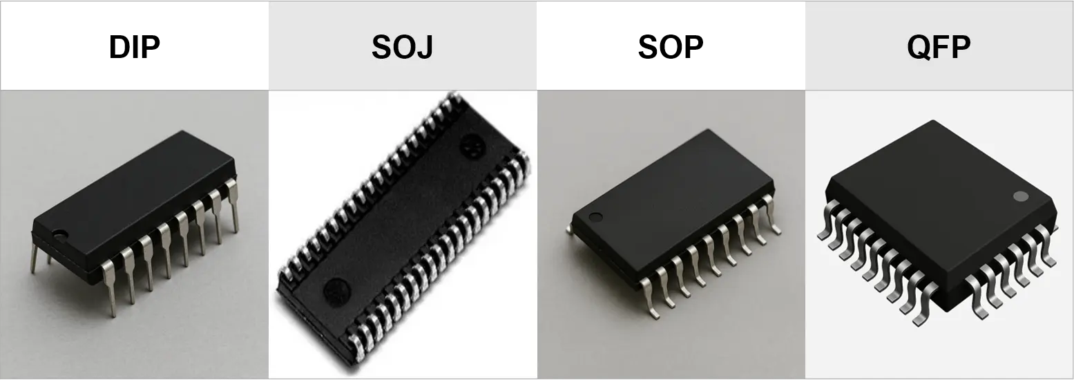
Example of an evaluatable package type
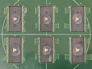
Even within these types, evaluation feasibility may vary depending on the shape and placement of the lead-frame.
De-capsulated TSSOP device
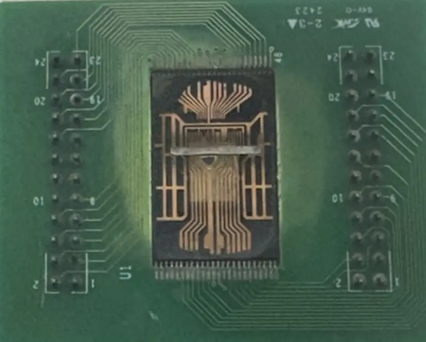
Non-Evaluatable Package Types
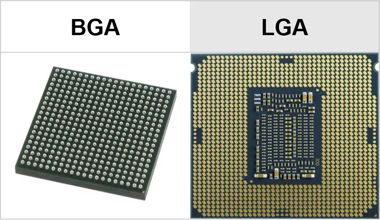
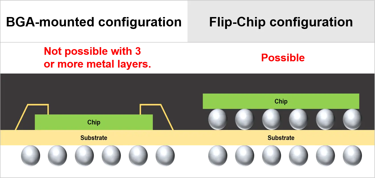
In packages like BGA, the bottom of the chip is fully bonded to the PCB via solder balls, allowing only top-side decapsulation. This generally makes back-side evaluation impossible.
Example of a non-evaluatable package type (1)
For BGAs where only the top side can be decapsulated, laser evaluation is often impractical for devices with more than three metal layers (e.g., memories, processors). However, some flip-chip BGA packages allow laser access from the bottom side of the die, enabling evaluation. In many cases, the same chip can be offered in multiple package options, selecting a laser-compatible package may make evaluation feasible.
Example of a non-evaluatable package type (2)
Preprocessing for Laser Radiation Hardness Testing
The examples above may not provide a definitive answer for every device. In most cases, X-ray imaging is used beforehand to inspect internal structures. Below are actual QRT case studies to help assess feasibility in similar situations.
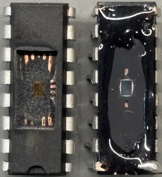
TSSOP Package (Memory, lead-frame removal not possible)
Front-side evaluation was blocked by the front-side metal stack. X-ray imaging showed the lead-frame was tied to multiple pins, preventing back-side frame removal. Even so, partial evaluation was carried out through gaps between lead-frame features, and potential SEE (Single Event Effects) were successfully detected.
Memory (TSSOP) back side
BGA & TSSOP Packages (Memory)
The original device was in BGA form, but a TSSOP version was acquired. Decapsulation was possible from both sides, but since the metal layer was covering the front-side, evaluation was conducted successfully from the back side.
Memory (TSSOP) back side
BGA Package (Memory)
Although BGA packages are generally difficult to evaluate, this particular flip-chip device allowed back-side laser access, enabling successful evaluation.
Front-side access was still restricted due to the ball grid array.
Memory (BGA) back side
TSSOP Package (Memory)
The lead-frame fully covered the back of the chip, requiring precise removal. Using detailed X-ray imaging and with support from the manufacturer, removable sections were identified.
Frame removal was performed successfully, exposing over 90% of the back-side die area for evaluation. Front-side evaluation remained blocked by the metal layer.
Memory (TSSOP) back side
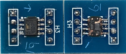
SOIC-8 Package (Op-Amp)
This simple SOIC-8 device was easily decapsulated and evaluated from both front and back.
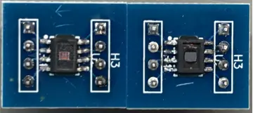
Op-Amp (SOIC) front (left), back (right)
PDIP Package (ADC)
The ADC, housed in a basic DIP package, was also easily decapsulated and evaluated on both sides.
ADC (PDIP) front (left), back (right)
SOIC-8 Package (Digital Isolator, partial lead-frame removal)
For the digital isolator, full front-side decapsulation caused damage to the internal coil. Selective decapsulation was performed to avoid interference with the coil.
The back-side lead-frame was connected to multiple pins, but careful partial removal enabled evaluation from both sides.
Digital Isolator (SOIC) front (left), back (right)